PCB Exposure Box
| date: | June 10, 2010 |
|---|
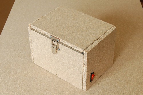
This summer I finaly decided to start making my own PCBs. The preferred method for making PCBs at home is photolithography. The PCBs used have a layer of photo resist, which is exposed to a source of light through a mask. The exposed areas are then removed using a special developer chemical. Lastly, the PCB is dipped into the etchant and the copper is removed from the areas unprotected by the photoresist.
The first thing I needed was a light source. I decided to build a small box for exposing my PCBs.
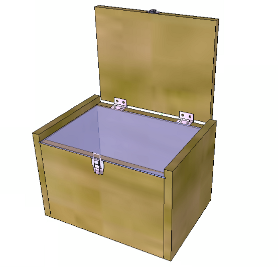
3D modeling
I began by creating a 3D model of the box usign Google Sketchup. This allowed me to spot any mistakes and tailor the design to suit my needs.
Bill of materials
I used the following parts to make this box:
- Chipboard
- Plexiglass for the window
- Fluorescent lamp
- Reflector from some old lamp
- IEC socket and cable
- Power switch
- Latch
- Pair of hinges
- Sponge cloth
- Screws, glue
Results
Below is the picture of a test PCB. The safe limit of track width seems to be around 0.2-0.25mm. This could be influenced by the source of light. While experimenting with the timing, I got an impression that UV light could do a better job as it would allow reduced exposure times.
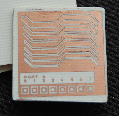
Track widths from top to bottom are:
- 1.27mm
- 0.64mm
- 0.38mm
- 0.25mm
- 0.20mm
- 0.15mm
- 0.10mm